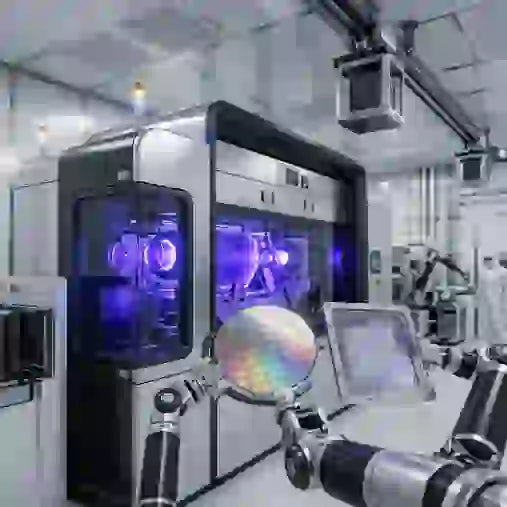
Silicon carbide JFET fabrication marks a significant evolution in technology, especially as Kyoto University and Phenitec Semiconductor successfully demonstrated the full-wafer batch fabrication of six-inch silicon carbide JFETs for extreme environments. This breakthrough, presented at the International Conference on Silicon Carbide and Related Materials in September 2026, bridges the gap between university prototypes and commercial semiconductor production.
The joint effort focuses on overcoming the drawbacks of conventional silicon-based integrated circuits, which typically degrade when exposed to high temperatures or intense radiation. Silicon carbide, known for its wide bandgap, is recognized as an excellent candidate for devices operating in harsh environments such as aerospace propulsion, nuclear monitoring, and planetary exploration. Traditional silicon carbide MOSFETs struggle under thermal stress due to the instability of their gate oxide layers. Therefore, the team innovatively leveraged junction field-effect transistors (JFETs), which use a semiconductor pn-junction instead of a gate oxide. This design choice enhances both thermal and radiation stability, crucial for reliable operation.
Another milestone was transferring this advanced device design to Phenitec Semiconductor's industrial production lines, showcasing how complex silicon carbide integrated circuits can be deployed using standard semiconductor equipment. By refining ion implantation and device isolation processes, the research group efficiently produced n-channel and p-channel JFETs across an entire six-inch wafer. Electrical tests verified uniform threshold voltage distribution and robust switching capabilities, essential for constructing complementary logic circuits similar to the widely used CMOS designs but fit for much harsher conditions.
The successful batch fabrication of silicon carbide JFETs underscores the feasibility of producing low-power, reliable circuitry for usage in the most challenging scenarios on Earth and beyond. As industries demand more durable and efficient electronics for extreme environments, this achievement positions silicon carbide technology as a cornerstone for future innovations.