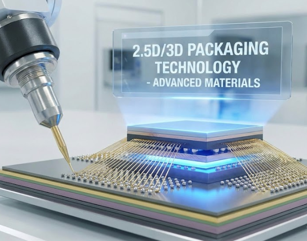
In a strategic move to address the soaring global demand for high-performance semiconductors, particularly those utilizing chiplet integration, NGK INSULATORS, LTD. (NGK) announced in November 2025 its plan to triple the production capacity of its "Hi-Ceram Carrier" by fiscal year 2027. The Hi-Ceram Carrier is a crucial support wafer used to temporarily hold and stabilize semiconductor chips during the advanced process of chiplet assembly.
The chiplet integration technology, which involves combining multiple smaller, specialized semiconductor chips (chiplets) into a single, high-performance package, is rapidly becoming the new standard for achieving performance gains beyond traditional monolithic chip scaling. This approach is essential for powering high-demand applications such as generative Artificial Intelligence (AI), High-Performance Computing (HPC), and autonomous driving. The global chiplet market is projected for massive growth, reflecting the urgency of this capacity expansion.
The Hi-Ceram Advantage: Quality and Durability
The Hi-Ceram Carrier distinguishes itself from conventional glass support wafers by utilizing NGK's proprietary translucent ceramic material, "Hi-Ceram." This material provides several distinct advantages:
-
High Rigidity and Durability: The ceramic structure ensures exceptional mechanical strength, which significantly reduces warpage and potential breakage of delicate semiconductor chips during manufacturing processes involving high temperatures and high loads.
-
Improved Yield and Process Stability: By minimizing the physical issues often associated with glass carriers, the Hi-Ceram Carrier enhances process stability for manufacturers, leading to higher product quality and a reduction in product loss.
-
Translucence: The material's light-transmitting properties are maintained, which can be critical for certain manufacturing steps.