SOKA TECHNOLOGY
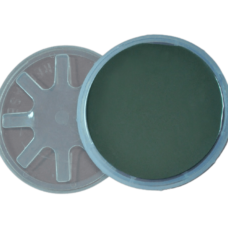
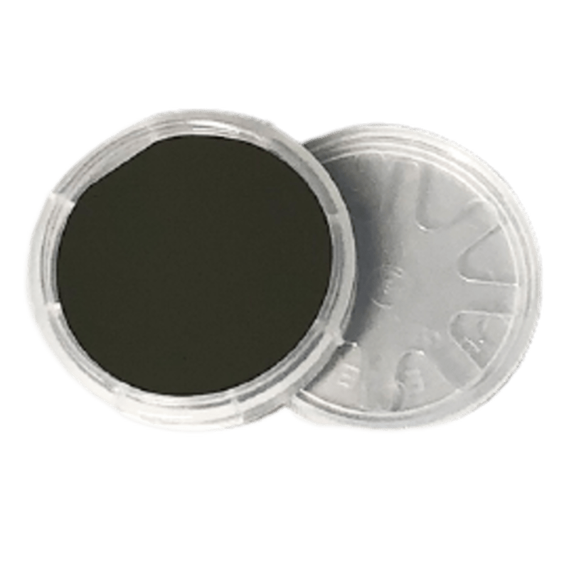
InP Substrate 2inch Semi-insulating 111B Indium Phosphide Semiconductor Wafer
オプションを選択
♦️High-quality InP wafer for Research and Experiment.
♦️Provide small quantities, special specifications products, and customized services
♦️Global shipping, secure payment, large inventory.
♦️Minimum delivery time within 1 week. Shipped by FedEx, DHL,UPS, etc.
Indium Phosphide (InP) Specification:
- Size: 2inch ;
- Diameter: 50.05mm±0.2 ;
- Dopant: S-C-N/S ;
- Thickness: 350um±25 ;
- Flat Option: EJ;
- Primary Orientation: [0-1-1]±0.02° ;
- Primary Flat Length: 16mm±2 ;
- Second Flat Orientation: [0-11] ;
- Second Flat Length: 7mm±1 ;
- Carrier Concentration: 2E18~8E18cm-3;
- Resistivity: 0.6E-3~2.5E-3Ω;
- Mobility: 1000~2000cm2/V·Sec;
- EPD: Ave<5000cm-2;
- Edge Rounding:0.25mmR(Conform to SEMI Standards);?
- TTV/TIR:≤10um ;
- BOW:≤10um ;
- Warp:≤15um ;
- Front side: Polished ;
- Backside: Etched;
- Epi-Ready: Yes ;
- Packing: Wafer case ;
当社には 7 日間の返品ポリシーがあり、商品を受け取ってから 7 日以内に返品をリクエストしてください。
返品の対象となるには、製品が未開封の場合はレシートまたは購入証明書をご提供ください。製品が開封されている場合は、製品の写真をご提供ください。
返品を開始するには、 info@sokatec.comまでご連絡ください。返品が受け付けられた場合は、返送用ラベルと、荷物の送り先と方法に関する指示をお送りします。返品のリクエストをせずに当社に返送された商品は受け付けられません。返品商品到着後3営業日以内にご返金させていただきます。返品費用は購入者が負担します。
返送先住所:中国上海市楊浦区平涼路1090号403号室。
ご質問がございましたら、いつでもinfo@sokatec.comまでご連絡ください。
損害と問題
ご注文を受け取ったらご確認いただき、商品に欠陥、破損、または間違った商品が届いた場合は、直ちにご連絡ください。問題を評価して適切な対応をさせていただきます。
例外・返品不可商品
生鮮品 (食品、花、植物など)、カスタム製品 (特注品やパーソナライズされた商品など)、パーソナルケア用品 (美容製品など) など、特定の種類の商品は返品できません。また、危険物、引火性液体、ガスなどの場合の返品も受け付けておりません。特定の商品についてご質問やご不明な点がございましたら、お気軽にお問い合わせください。
申し訳ございませんが、セール品やギフトカードの返品はお受けできません。
交換
欲しいものを確実に手に入れる最も早い方法は、お持ちの商品を返品し、返品が受け入れられたら、新しい商品を別途購入することです。
払い戻し
返品を受領して検査した後、返金が承認されたかどうかをお知らせします。承認された場合は、元のお支払い方法で自動的に返金されます。銀行やクレジット カード会社が返金を処理して掲載するまでにも時間がかかる場合があることに注意してください。
連絡先
ソウカテクノロジー株式会社
住所:東京都台東区上野5-16-16天美ビル2階6号室
WeChat: +1-3152162986
Whatsapp: +81-7090566595
問い合わせ先:ション/電話:+81-368203586
メール:info@sokatec.com
Products
1.What products does the company mainly provide?
- Semiconductor substrates
- Solar energy products
- Ceramics products
- Processing services
2.Where do the company's products and services come from?
Our partners mainly include the United States, Germany, Japan, China and other countries and regions. In addition to stock products, we can also provide customized processing services
Shipping
1.Do you ship worldwide?
Yes, we ship worldwide and We use Fedex, DHL and other express companies.
2. Where you ship goods from ?
Normally we ship the goods from China. meanwhile we have also warehouse in Japan. It depends on the situation as needs.
3.What is the shipping cost ?
The freight in North America is generally US$129
The shipping fee in Asia,South America and Europe is generally 30-50 US dollars
Free shipping for products purchased above a certain amount, please contact us for details
E-mail: info@sokatec.com
4. What is the shipping time ?
The time frame for order delivery is divided into two parts:
- Processing time: Order verification, tailoring, quality check and packaging. All orders are sent to the manufacturers for dispatch within 24 hours after the order is placed. If the products are in stock, which takes an additional 2–4 days (except holidays).
- Shipping time: We use Fedex, DHL and other express companies, and the shipping time is generally 4-6 days.
5. How do I track my package?
You can track your parcel via the Confirmation Email. Also, you can click “Track my Order” link on our website.
Payment & Ordering
1.What payment terms you can accept?
We can accept Paypal, Google Pay, Apple Pay, Visa, Mastercard, and American Express.
We can also accept bank transfers, including USD, EUR, GBP, JPY, KRW, etc.
2. My payment was declined, why?
If your credit card is declined there may be a few reasons why: the card has no funds available, you entered the wrong CSV security code, the card is expired, you entered the wrong billing information, the card does not allow internet purchases (card not present purchases), there is a hold on the card. In any event by calling your issuing bank they can tell you why the card is declining.
Solutions: try a different credit card or try using PayPal as your checkout method (they accept VISA, MasterCard, American Express and Diners Club.
3.How do I cancel my order?
Only unshipped orders may be cancelled. Cancellation may be done either through email or by telephone. Refund will be issued accordingly if card is charged.
4. Is my information is securing using this site?
Absolutely!!! Our Secure Software (SSL) is the industry standard and among the best software available today for secure commerce transactions. It encrypts your credit card number so that it cannot be read as the information travels over the Internet.
5.What if my address is wrong?
If your dress is not available, we will send you an email and/or call you. Please be sure to check your email within 24 hours of placing your order. We will do everything we can to fufill your order.
Return & Refunds
1.What items are returnable?
- Within 7 days of after receiving goods
- Products with quality problems
2.How do I return a product?
Once you have alerted us you wish to make a return through an email contact. We will contact you to start the return process.
E-mail: info@sokatec.com
3. What is your refund policy?
Our complete return policy is located at the RETURNS link at the bottom of the site
4.How will you refund me ?
You can find our refund policy by the link The refund will go back onto the same card you used to place the order with us, and will be paid back to you via a return transaction. Please allow 3-5 days for the funds to show in your account.
Contact us

America
Contact: Sophie
sophie@sokatec.com
Tel:+1-6463916255

England
Contact: Elsa
elsa@sokatec.com
Tel:+44-7972294236

Germany
Contact: Shan
shan@sokatec.com
Tel:+49-17647655770
Japan
Contact: Shon
sales@sokatec.com
Tel:+81-368203586

Korea
Contact: Kim
kim@sokatec.com
Tel:+82-1090065688

India
Contact: Chraiseto
chraiseto@sokatec.com
Tel:+91-9488669046
