SOKA TECHNOLOGY
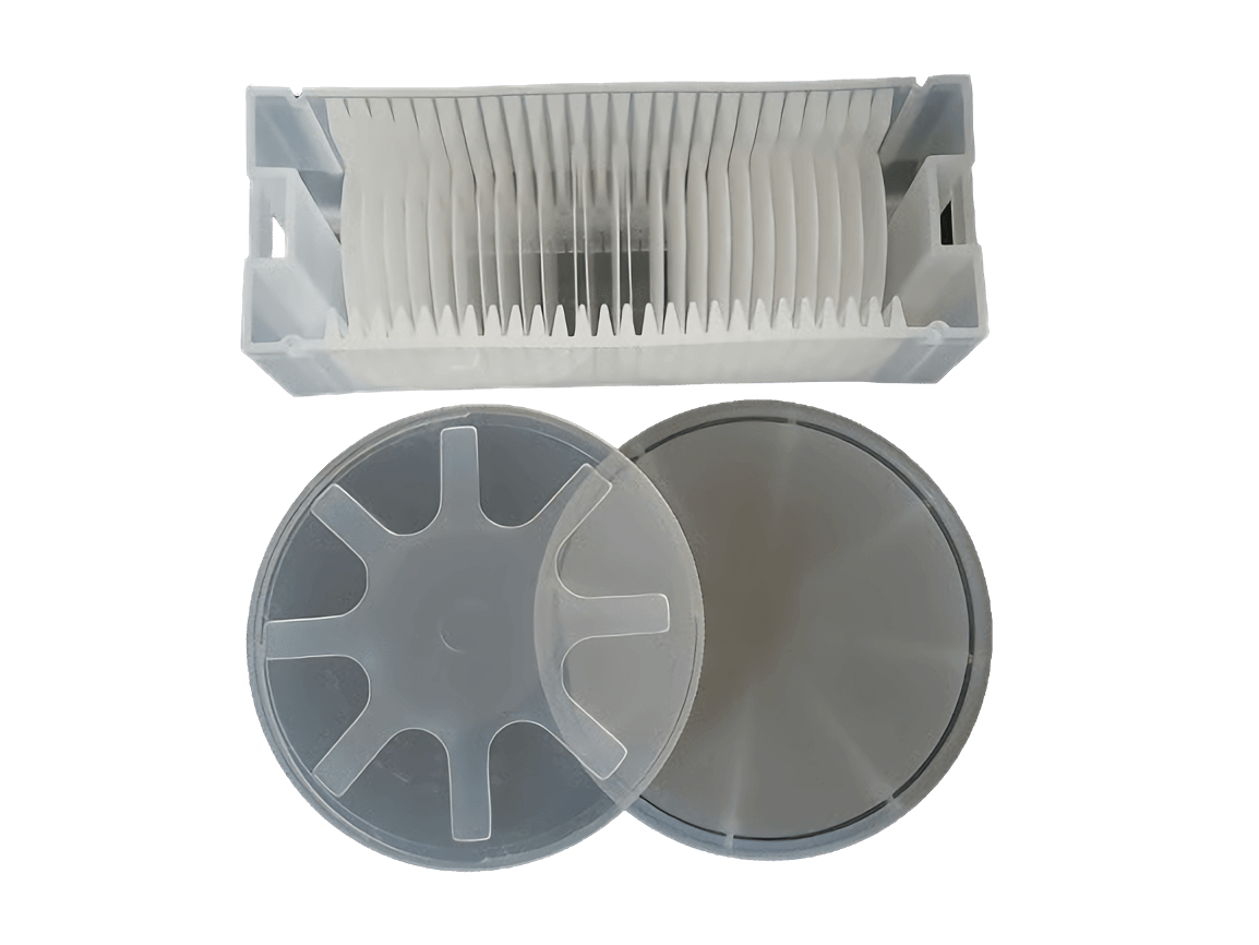
Lithium Niobate Substrate 4inch Y-Cut 128º DSP SAW Acoustic Optics Grade LN LiNbO3 Wafer
Choose options
♦️High-quality LN wafer for Research and Experiment.
♦️Provide small quantities, special specifications products, and customized services
♦️Global shipping, secure payment, large inventory.
♦️Minimum delivery time within 1 week. Shipped by FedEx, DHL,UPS, etc.
LiNbO3(LN) Substrate Specification:
- Size: 4inch;
- Method: CZ;
- Diameter: 100 ± 0.5mm;
- Thickness: 500um ± 25;
- Orientation: 128º Rotated Y-axis;
- TTV<10um;
- Front side: polished;
- Backside: polished;
- Packing: Wafer case + clean pack;
We have a 7-day return policy, which means you have 7 days after receiving your item to request a return.
To be eligible for a return, If the product has not been opened, please provide the receipt or proof of purchase.If the product has been opened, please provide a photo of the product.
To start a return, you can contact us at info@sokatec.com. If your return is accepted, we’ll send you a return shipping label, as well as instructions on how and where to send your package. Items sent back to us without first requesting a return will not be accepted. We will refund the payment within 3 working days after receiving the returned goods. The return cost is paid by the buyer.
Return address: 6-5 Tokyo Danchi Warehouse North Building, 6-2-11 Iriya, Adachi-ku, Tokyo 121-0836, Japan
You can always contact us for any return question at info@sokatec.com.
Damages and issues
Please inspect your order upon reception and contact us immediately if the item is defective, damaged or if you receive the wrong item, so that we can evaluate the issue and make it right.
Exceptions / non-returnable items
Certain types of items cannot be returned, like perishable goods (such as food, flowers, or plants), custom products (such as special orders or personalized items), and personal care goods (such as beauty products). We also do not accept returns for hazardous materials, flammable liquids, or gases. Please get in touch if you have questions or concerns about your specific item.
Unfortunately, we cannot accept returns on sale items or gift cards.
Exchanges
The fastest way to ensure you get what you want is to return the item you have, and once the return is accepted, make a separate purchase for the new item.
Refunds
We will notify you once we’ve received and inspected your return, and let you know if the refund was approved or not. If approved, you’ll be automatically refunded on your original payment method. Please remember it can take some time for your bank or credit card company to process and post the refund too.
Contact Information
SOKA TECHNOLOGY LTD
Address: No.6, 2F, Tenbi Building, 5-16-16, Ueno,Taito-ku, Tokyo,Japan
Wechat: +1-3152162986
Whatsapp: +1-3152162986
Contact: Shon/Call:+81-0368203586
Email:info@sokatec.com
Products
1.What products does the company mainly provide?
- Semiconductor substrates
- Solar energy products
- Ceramics products
- Processing services
2.Where do the company's products and services come from?
Our partners mainly include the United States, Germany, Japan, China and other countries and regions. In addition to stock products, we can also provide customized processing services
Shipping
1.Do you ship worldwide?
Yes, we ship worldwide and We use Fedex, DHL and other express companies.
2. Where you ship goods from ?
Normally we ship the goods from China. meanwhile we have also warehouse in Japan. It depends on the situation as needs.
3.What is the shipping cost ?
The freight in North America is generally US$129
The shipping fee in Asia,South America and Europe is generally 30-50 US dollars
Free shipping for products purchased above a certain amount, please contact us for details
E-mail: info@sokatec.com
4. What is the shipping time ?
The time frame for order delivery is divided into two parts:
- Processing time: Order verification, tailoring, quality check and packaging. All orders are sent to the manufacturers for dispatch within 24 hours after the order is placed. If the products are in stock, which takes an additional 2–4 days (except holidays).
- Shipping time: We use Fedex, DHL and other express companies, and the shipping time is generally 4-6 days.
5. How do I track my package?
You can track your parcel via the Confirmation Email. Also, you can click “Track my Order” link on our website.
Payment & Ordering
1.What payment terms you can accept?
We can accept Paypal, Google Pay, Apple Pay, Visa, Mastercard, and American Express.
We can also accept bank transfers, including USD, EUR, GBP, JPY, KRW, etc.
2. My payment was declined, why?
If your credit card is declined there may be a few reasons why: the card has no funds available, you entered the wrong CSV security code, the card is expired, you entered the wrong billing information, the card does not allow internet purchases (card not present purchases), there is a hold on the card. In any event by calling your issuing bank they can tell you why the card is declining.
Solutions: try a different credit card or try using PayPal as your checkout method (they accept VISA, MasterCard, American Express and Diners Club.
3.How do I cancel my order?
Only unshipped orders may be cancelled. Cancellation may be done either through email or by telephone. Refund will be issued accordingly if card is charged.
4. Is my information is securing using this site?
Absolutely!!! Our Secure Software (SSL) is the industry standard and among the best software available today for secure commerce transactions. It encrypts your credit card number so that it cannot be read as the information travels over the Internet.
5.What if my address is wrong?
If your dress is not available, we will send you an email and/or call you. Please be sure to check your email within 24 hours of placing your order. We will do everything we can to fufill your order.
Return & Refunds
1.What items are returnable?
- Within 7 days of after receiving goods
- Products with quality problems
2.How do I return a product?
Once you have alerted us you wish to make a return through an email contact. We will contact you to start the return process.
E-mail: info@sokatec.com
3. What is your refund policy?
Our complete return policy is located at the RETURNS link at the bottom of the site
4.How will you refund me ?
You can find our refund policy by the link The refund will go back onto the same card you used to place the order with us, and will be paid back to you via a return transaction. Please allow 3-5 days for the funds to show in your account.
Contact us

America
Contact: Sophie
sophie@sokatec.com
Tel:+1-6463916255

England
Contact: Elsa
elsa@sokatec.com
Tel:+44-7972294236

Germany
Contact: Shan
shan@sokatec.com
Tel:+49-17647655770
Japan
Contact: Shon
sales@sokatec.com
Tel:+81-368203586

Korea
Contact: Kim
kim@sokatec.com
Tel:+82-1090065688

India
Contact: Chraiseto
chraiseto@sokatec.com
Tel:+91-9488669046

Vietnam
Contact: Hieuoggy
nguyen@sokatec.com
Zalo:+84-915750102
