SOKA TECHNOLOGY
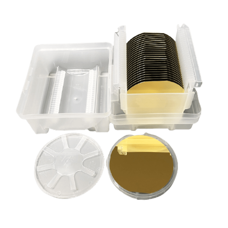
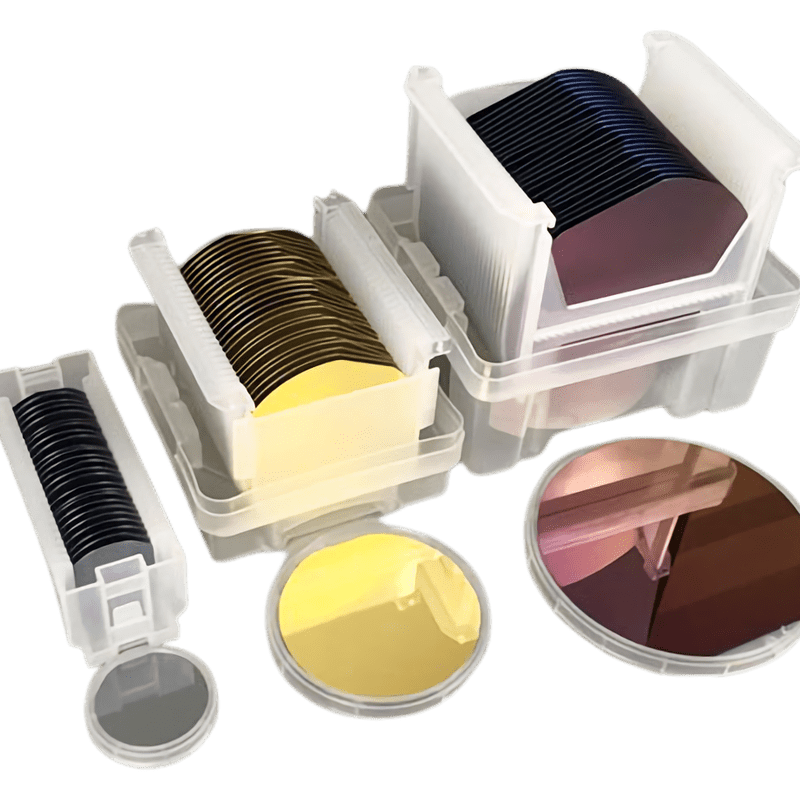
シリコンウェーハ 4inch P型(100) 0.005-0.01Ω ニッケル層 半導体基板
オプションを選択
♦️ 研究・実験用の高品質シリコンウェハー。
♦️ 少量提供、特別仕様製品、カスタマイズサービスに対応.
♦️国際配送、安心の支払い、大量在庫.
♦️最短1週間以内の納期。FedEx、DHL、UPS等で出荷。
金属層ウェハー 仕様:
- サイズ: 4inch;
- 製法: CZ;
- タイプ: P;
- ドーパント: B;
- 方位: 100;
- 抵抗率: 0.005-0.01Ω;
- 厚さ: 525um±25;
- ニッケル層: 1000nm;
- TTV<10um ;
- 表面: 研磨済み;
- 裏面: エッチング済み;
- 梱包: シリコンウェハーケース ;
当店の返品ポリシーは7日間です。商品到着後7日以内に返品のご依頼をしてください。
返品の対象となるためには、未開封の商品についてはレシートまたは購入証明を、開封済みの商品については商品の写真をご提出ください。
返品を開始するには、 info@sokatec.comまでご連絡ください。返品が承認された場合、返送用の配送ラベルと、発送方法および送付先の指示をお送りします。事前に返品依頼を行わずに返送された商品は受け付けられません。 ご返送商品を受領後、3営業日以内にご返金いたします。返品送料は購入者負担です。
返品先住所: 6-5 Tokyo Danchi Warehouse North Building, 6-2-11 Iriya, Adachi-ku, Tokyo 121-0836, Japan
返品に関するご質問はいつでも info@sokatec.comまでご連絡ください。
破損や問題について
商品到着時に必ずご確認のうえ、商品の欠陥・破損、または誤配送があった場合は直ちにご連絡ください。問題を確認し、適切に対応いたします。
例外/返品不可の商品
以下のような商品は返品できません。生鮮品(食品、花、植物など)、カスタム商品(特注品や名入れ商品など)、および衛生用品(化粧品など)は対象外です。また、危険物、可燃性液体、ガス類の返品もお受けできません。特定の商品についてご不明点がある場合はお問い合わせください。
セール品やギフトカードの返品は承れませんので、あらかじめご了承ください。
交換について
ご希望の商品を確実に入手する最も早い方法は、一旦現物を返品していただき、返品が承認された後に改めて新しい商品を別途ご購入いただくことです。
返金について
返品商品を受領・検品した後、返金の可否をお知らせします。承認された場合は、ご購入時の支払方法へ自動的に返金されます。銀行やクレジットカード会社の処理に時間を要する場合があることをご了承ください。
お問い合わせ先
SOKA TECHNOLOGY LTD
住所: No.6, 2F, Tenbi Building, 5-16-16, Ueno,Taito-ku, Tokyo,Japan
Wechat: +1-3152162986
Whatsapp: +1-3152162986
担当: Shon/電話:+81-0368203586
メール:info@sokatec.com
Products
1.What products does the company mainly provide?
- 半導体基板
- 太陽エネルギー製品
- セラミック製品
- 加工サービス
2.Where do the company's products and services come from?
当社のパートナーは主にアメリカ、ドイツ、日本、中国などの国や地域を含みます。在庫製品に加えて、カスタム加工サービスも提供可能です。
Shipping
1.Do you ship worldwide?
はい、世界中へ発送いたします。当社はFedex、DHLなどの国際宅配便を利用しています。
2. Where you ship goods from ?
通常は中国から発送します。なお、状況に応じて日本の倉庫から発送することもあります。
3.What is the shipping cost ?
北米向けの送料は一般的にUS$129です
アジア、南米、ヨーロッパ向けの送料は一般的に30〜50米ドルです
一定金額以上のご購入で送料無料となる場合があります。詳細はお問い合わせください。
E-mail: info@sokatec.com
4. What is the shipping time ?
ご注文の配送にかかる期間は以下の2つに分かれます:
- 処理時間:注文の確認、加工、品質検査、梱包を指します。すべての注文は注文確定後24時間以内に出荷手配のため製造元へ送られます。在庫がある場合はさらに2~4日がかかります(祝日を除く)。
- 配送時間:当社はFedex、DHLなどの国際宅配便を利用しており、配送には通常4~6日かかります。
5. How do I track my package?
ご注文確定メールから荷物を追跡できます。また、当社ウェブサイトの「注文を追跡」リンクからもご確認いただけます。
Payment & Ordering
1.What payment terms you can accept?
当社はPaypal、Google Pay、Apple Pay、Visa、Mastercard、American Expressを受け付けます。
銀行振込も対応可能です(USD、EUR、GBP、JPY、KRW等)。
2. My payment was declined, why?
クレジットカードが拒否される理由はいくつか考えられます:残高不足、CSVセキュリティコードの誤入力、カードの有効期限切れ、請求先情報の誤入力、オンライン決済(カード非提示取引)を許可していないカード、カードに保留がかかっている場合。発行銀行にお問い合わせいただければ、拒否の理由がわかります。
Solutions: try a different credit card or try using PayPal as your checkout method (they accept VISA, MasterCard, American Express and Diners Club.
3.How do I cancel my order?
発送前の注文のみキャンセル可能です。キャンセルはメールまたは電話で行えます。カード決済済みの場合は、該当額を返金いたします。
4. Is my information is securing using this site?
もちろんです!当社のセキュアソフトウェア(SSL)は業界標準であり、現在利用可能な最高水準の安全な取引ソフトウェアの一つです。クレジットカード番号は暗号化され、インターネット上を移動する間に読み取られることはありません。
5.What if my address is wrong?
ご住所に不備がある場合は、メールおよび/または電話でご連絡いたします。ご注文後24時間以内にメールをご確認ください。ご注文を履行できるよう最善を尽くします。
Return & Refunds
1.What items are returnable?
- 商品受領後7日以内
- 品質に問題のある製品
2.How do I return a product?
返品をご希望の場合は、まずメールでご連絡ください。返品手続きを開始するために当方からご連絡いたします。
E-mail: info@sokatec.com
3. What is your refund policy?
当社の返品ポリシーはサイト下部のRETURN(返品)リンクに記載されています。
4.How will you refund me ?
返金はご注文時にご利用いただいたカードへ返金処理されます。返金が口座に反映されるまで3〜5日ほどかかる場合があります。
お問い合わせ

アメリカ
お問い合わせ: Sophie
sophie@sokatec.com
Tel:+1-6463916255

イングランド
連絡先: Elsa
elsa@sokatec.com
電話:+44-7972294236

ドイツ
お問い合わせ: Shan
shan@sokatec.com
電話:+49-17647655770
日本
お問い合わせ: Shon
sales@sokatec.com
Tel:+81-368203586

韓国
担当者:Kim
kim@sokatec.com
電話:+82-1090065688

インド
お問い合わせ: Chraiseto
chraiseto@sokatec.com
電話: +91-9488669046
